
For decades, the semiconductor industry treated cooling as the problem that happened after the chip was designed. Engineers optimized transistor density, clock speed, and memory bandwidth first. Thermal management came later bolted on, air-blown, and steadily outpaced. TSMC’s Silicon-Integrated Micro Cooler (IMC-Si) has ended that sequencing permanently.
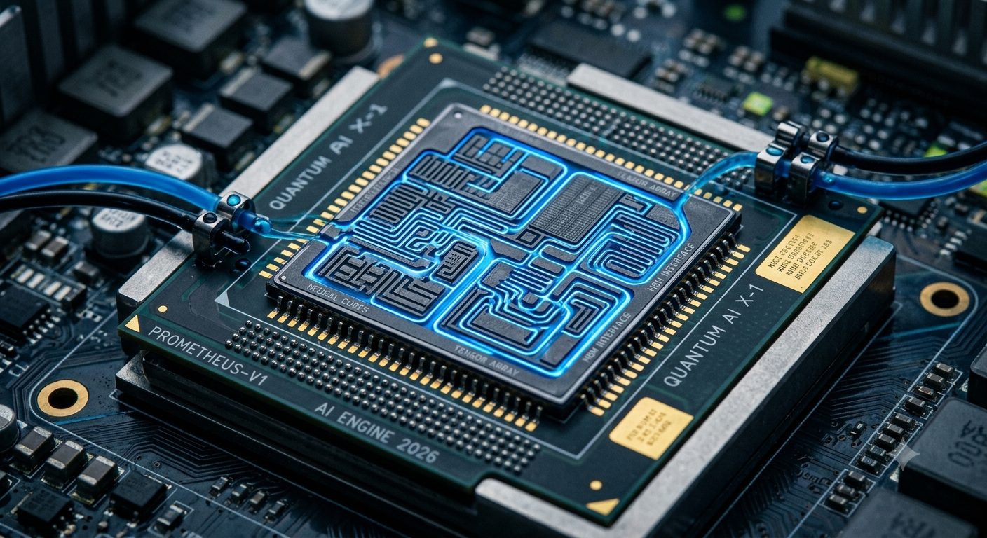
The announcement carries weight beyond its technical specifications. When TSMC presented the IMC-Si at the 2025 IEEE Electronic Components and Technology Conference, the company did not position it as a feature upgrade. Researchers described it as an architectural inevitability. The IMC-Si integrates microfluidic channels directly into the chip’s backside through TSMC’s CoWoS wafer-to-wafer bonding process meaning coolant now circulates within microns of active transistors, not centimeters away through an external cold plate.
The measured outcome: a thermal resistance of 0.055°C/W. That represents a 15% improvement over the most advanced external liquid cooling configurations available today. In a sector where marginal efficiency gains require multi-billion-dollar facility investments, a 15% thermal resistance reduction at the silicon level is not incremental. It restructures the entire thermal chain beneath it.
The Thermal Wall Was Always the Real Bottleneck
The phrase “thermal wall” has circulated in semiconductor circles for years, but the industry treated it as a distant constraint. NVIDIA’s Rubin architecture made it a present one. NVIDIA’s Blackwell B200 and GB200 series released across 2024 and 2025 pushed thermal design power into the 1,200W range. Engineers adapted. Copper cold plates, advanced thermal interface materials, and high-flow CDUs kept pace. However, the Rubin R100, unveiled at CES 2026 as the first mass-market processor to cross the 2,000W threshold, pushed TDP as high as 2,300W per GPU. At that power density, the Thermal Interface Material the microscopic layers of paste and solder between chip and cooler became the bottleneck, not the cooling loop itself.
TSMC’s IMC-Si removed that bottleneck by eliminating the interface entirely. Validated on a 3,300mm² CoWoS interposer supporting multiple logic dies and HBM stacks, chips running on the IMC-Si architecture sustained above 2.6kW TDP while remaining below 63°C a junction temperature once considered unachievable for 3D chip configurations. Dr. Kevin Zhang, TSMC’s Deputy Co-COO and Senior VP, stated the strategic intent directly: “Direct-to-Silicon Liquid Cooling breaks the thermal wall, unlocking the full potential of CoWoS for exascale AI. This isn’t just incremental; it’s transformative for sustainable computing.” That framing matters. Zhang did not describe IMC-Si as a cooling innovation. He described it as an AI infrastructure enabler. The distinction signals a shift in how TSMC understands its own role in the compute value chain.
AWS Proved the Commercial Case Before the Industry Caught Up
While TSMC addressed the silicon layer, AWS validated what happens when liquid cooling redesigns the entire data center stack. At AWS re:Invent, Amazon unveiled next-generation data center designs featuring jointly developed liquid cooling solutions built around NVIDIA’s GB200 NVL72 rack-scale architecture. The results, stated by AWS directly: a 12% increase in compute power per site and a reduction in mechanical energy consumption by up to 46% during peak cooling conditions with no additional water consumption required.
AWS developed its custom liquid cooling solution, including a proprietary in-row coolant distribution unit, in approximately 11 months. The system supports NVIDIA Trainium2 and GB200 NVL72 chipsets and is retrofittable meaning AWS can apply the architecture to existing facilities, not only new builds. The company reported a global Power Usage Effectiveness (PUE) of 1.15 in 2024. The 46% mechanical energy reduction is not a projected figure. It applies during peak cooling conditions — historically the highest-cost operational window for any hyperscale facility. The new electrical distribution system that accompanies the cooling redesign reduces potential failure points by up to 20% by minimizing electrical conversion steps and relocating backup power sources closer to server racks.
This is not a sustainability story dressed as an infrastructure story. This is an economics story. AWS is extracting 12% more compute from the same physical site footprint while simultaneously cutting the energy overhead that accounts for approximately 40% of total data center operating costs.
The Supply Chain Has Not Caught Up to the Physics
The technical achievements of TSMC and AWS clarify something the broader industry has been reluctant to confront: the infrastructure supply chain is structurally misaligned with where compute density is heading. TSMC’s CoWoS packaging capacity remains constrained. Major customers, including NVIDIA, secure allocations well in advance, with current bookings extending into 2026-27. Smaller operators face either premium pricing or extended lead times. The IMC-Si architecture, integrated into the CoWoS manufacturing process, is not available as a retrofit it must be designed in from wafer production. Operators who cannot secure Rubin-generation hardware with embedded cooling will run increasingly thermally limited workloads on facilities designed around yesterday’s heat assumptions.
Meanwhile, the cooling vendor ecosystem CDU manufacturers, cold plate suppliers, dielectric fluid producers is scaling rapidly but from a low base. Goldman Sachs forecast that liquid-cooled AI servers would represent 76% of deployments by 2026, up from 15% in 2024. That pace of adoption leaves little margin for supply chain lag. NVIDIA’s participation in the U.S. Department of Energy’s COOLERCHIPS program a federally backed initiative projected to reduce costs by at least 5% and improve efficiency by 20% over traditional air-cooled designs signals that the thermal problem at this scale now draws government-level attention. Cooling is no longer a vendor conversation. It is an energy policy conversation.
What This Means for Operators, Investors, and Policymakers
The combined signal from TSMC’s IMC-Si and AWS’s liquid-cooled next-generation facilities is not ambiguous. Thermal management has become the primary design constraint in AI infrastructure not power availability, not land, not fiber connectivity. For data center operators, the architectural implication is direct: facilities designed around 20kW average rack densities cannot serve AI training clusters without major mechanical plant replacement. TSMC’s direct-to-silicon approach locks thermal architecture decisions into the chip fabrication process, meaning operators must align their facility designs with GPU roadmaps two to three years ahead of deployment or accept performance compromises that undercut the economics of AI workloads entirely.
For investors, the thermal chain is now a value chain. Companies positioned across CDU manufacturing, dielectric fluid supply, and silicon-level thermal engineering hold structural leverage in the AI buildout that chip designers alone cannot replicate. For policymakers particularly in markets such as India, where data center capacity is projected to grow from 1.5GW to 8-10GW by 2030 the efficiency outcomes demonstrated by TSMC and AWS carry direct relevance to water and energy policy. A 46% reduction in mechanical cooling energy at AWS scale, replicated across a national data center buildout, represents a material difference in grid demand and water consumption projections.
The thermal wall, as TSMC has now demonstrated, is solvable. Whether the industry moves fast enough to solve it at the infrastructure layer before facility commitments, energy contracts, and water permits lock in the assumptions of an older thermal era is the question that will define the next five years of AI compute.


