Coverage of the TPU 8t and TPU 8i announcement at Google I/O 2026 has focused on hardware. In reality, Google told an infrastructure story. By splitting training and inference into two purpose-built silicon architectures, Google is not primarily pursuing better chip performance. It is redefining how operators design facilities for those chips, which workloads those facilities must support simultaneously, and how the infrastructure investment required to serve training and inference at Google’s scale differs from the investment a single-chip architecture would require. Understanding those differences is the starting point for understanding what the dual-TPU architecture means for AI infrastructure design beyond Google’s own campuses.
Training and inference have been recognised as distinct workload types since the beginning of the deep learning era. What has changed is the scale at which each needs to be served and the degree to which optimising for one involves compromising the other. Training requires synchronised access across millions of chips simultaneously, maximum inter-chip bandwidth, tolerance for batch processing latency, and thermal and power infrastructure designed for continuous maximum-utilisation operation. Inference requires the opposite: low per-request latency, high concurrency for simultaneous user requests, on-chip memory large enough to cache the KV state of active sessions, and power infrastructure designed for highly variable load profiles that surge when user traffic peaks and drop when it doesn’t.
The Facility Design Implications
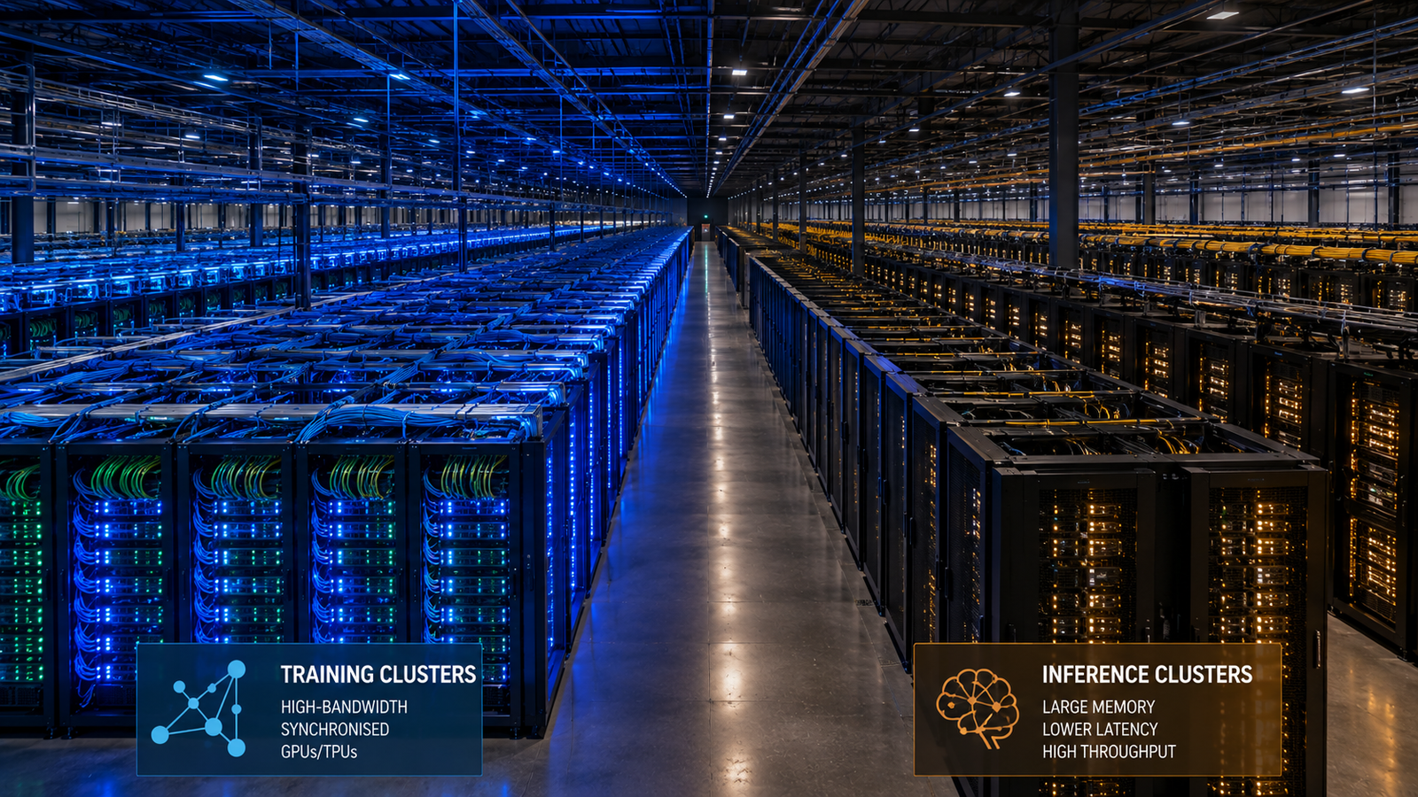
A facility designed to optimise for training workloads looks different from a facility designed to optimise for inference workloads in specific and commercially significant ways. Training facilities benefit from maximum power density per rack, direct liquid cooling at the highest available coolant temperatures, very high inter-rack network bandwidth, and physical proximity of racks within a training cluster to minimise latency across the synchronised compute fabric. Inference facilities benefit from higher concurrency per watt, more rack-level memory capacity relative to compute capacity, and networking optimised for serving many simultaneous requests rather than synchronising a single massive computation.
The TPU 8i’s 384MB of on-chip SRAM and 288GB of HBM — dramatically more memory than a training-optimised chip needs — are designed specifically for inference KV cache requirements. Holding large KV caches in silicon eliminates the latency of reading cache from DRAM on every inference request. That memory architecture changes the facility’s power and cooling requirements, because a chip carrying 288GB of HBM has different thermal output characteristics and different power delivery requirements from a chip optimised for raw compute throughput. A facility that mixes training and inference hardware at scale will need zone-level power and cooling differentiation that uniform-architecture facilities do not require.
What This Means for the Neocloud Market
The dual-TPU architecture creates a specific challenge for neocloud operators that built their infrastructure around GPU fleets serving both training and inference workloads. One of the core commercial advantages of GPU-based neocloud infrastructure has been the ability to redirect the same hardware between training and inference as customer demand shifts. By optimising separate chips for each workload type, a dual-chip architecture improves performance per dollar for both, but sacrifices the flexibility that a unified architecture delivers.
For a neocloud operator evaluating whether to build TPU-based or GPU-based infrastructure, the dual-chip architecture raises a specific operational question: how stable is the training-to-inference ratio in the customer workload mix, and does the performance advantage of purpose-built hardware for each workload type justify the operational complexity of managing two separate hardware ecosystems? CoreWeave’s $99 billion backlog is built on GPU infrastructure that serves both workload types. The Google-Blackstone TPU cloud venture, which we examined in our analysis of Nvidia’s infrastructure dominance challenge, will need to address that flexibility question directly as it competes for enterprise customers whose workload mixes vary significantly across deployment types and development stages.
The Long-Term Infrastructure Architecture Question
The dual-TPU architecture is the clearest signal yet that the AI infrastructure market is moving toward specialised facilities rather than general-purpose AI data centers. If the industry’s leading infrastructure investor, a company spending $190 billion per year on AI infrastructure, has determined that training and inference require separate silicon architectures, the logical next step is to build separate facility architectures for each. Training campuses designed for maximum power density, synchronised inter-chip bandwidth, and continuous maximum-utilisation operation. Inference campuses designed for high concurrency, memory-rich architectures, and variable load profiles.
The same bifurcation that the dual-TPU architecture introduces at the silicon level will propagate upward into facility design, site selection, power procurement, and operational models as the scale of AI infrastructure deployment makes that specialisation economically justified. The operators who design for that specialisation now are building facilities that will remain competitive through multiple hardware generations. The ones designing for today’s GPU-centric general-purpose model are building facilities that will need to adapt as the architecture evolves.
Hardware Specialisation Will Redefine Facility Design
The economics of specialisation become increasingly compelling as hardware generations advance. The gap in optimal facility requirements between a training chip and an inference chip will widen with each successive generation as the performance-per-watt optimisation logic for each workload type pushes the silicon further from the generalist design point. By the time Rubin-class training hardware and its inference equivalent arrive, the optimal facility for each may share only their grid connection and physical security requirements. The operators building training-inference hybrid facilities today are building for the hardware of 2026. The operators thinking about what a pure inference facility needs in 2028 are building for the market that Google’s dual-TPU architecture has just described. The architecture question that seemed theoretical two years ago is now a construction specification.
The broader implication for the AI infrastructure market extends beyond facility design to the competitive dynamics between cloud providers, neoclouds, and enterprise operators. A hyperscaler that runs both training and inference at scale can justify the operational complexity of two hardware ecosystems because it has the volume to make each viable independently. A neocloud that serves primarily inference customers can justify building pure inference infrastructure and achieving the cost per useful token that specialised hardware and facility design enables. An enterprise running primarily internal inference workloads has no training workload to balance against, which means the dual-chip architecture makes on-premise AI inference infrastructure more economically viable than it was when training and inference shared the same hardware generation. Google’s architectural decision at I/O 2026 will influence data center design specifications, steer vendor product roadmaps, and reshape enterprise IT procurement decisions over the next five years.


